

Mastering Prototype PCB Assembly Processes with pcb assembly services ventura
- AES

- Jun 16
- 3 min read
Prototype PCB assembly is a critical step in the development of electronic products. It bridges the gap between design and full-scale production. Mastering this process ensures that the final product meets quality, functionality, and reliability standards. I will share practical insights and actionable steps to help you navigate prototype PCB assembly efficiently. This knowledge is essential for companies in aerospace, medical devices, consumer electronics, and defense sectors.
Understanding the Importance of pcb assembly services ventura
Choosing the right PCB assembly service is the foundation of a successful prototype. The process involves placing and soldering components on a printed circuit board to create a functional prototype. This step validates the design and identifies potential issues early.
In Ventura, specialized pcb assembly services ventura offer tailored solutions for complex and high-reliability applications. These services provide:
Quick turnaround times to meet tight development schedules
Expertise in handling advanced components and fine-pitch parts
Compliance with industry standards such as IPC-A-610 and ISO certifications
Access to advanced equipment like automated pick-and-place machines and reflow ovens
Selecting a service provider with these capabilities reduces risk and accelerates time to market.
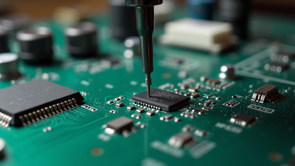
Key Steps in Prototype PCB Assembly
Mastering prototype PCB assembly requires a clear understanding of each step. Here is a breakdown of the essential stages:
1. Design Review and DFM Analysis
Before assembly, review the PCB design for manufacturability. Design for Manufacturability (DFM) analysis identifies potential issues such as:
Component placement conflicts
Inadequate solder mask clearance
Incorrect pad sizes or footprints
Addressing these early prevents costly rework.
2. Material Procurement and Component Verification
Ensure all components meet specifications and are sourced from reliable suppliers. Verify component authenticity and check for any counterfeit parts. This step is crucial for high-reliability sectors like aerospace and defense.
3. Stencil Preparation and Solder Paste Application
A precision stencil applies solder paste to the PCB pads. The quality of the stencil and the accuracy of paste application directly affect solder joint integrity.
4. Component Placement
Automated pick-and-place machines position components on the PCB. For prototypes, manual placement may be necessary for complex or low-volume parts.
5. Soldering Process
Reflow soldering is the most common method for surface mount technology (SMT). For through-hole components, wave soldering or manual soldering may be used.
6. Inspection and Testing
Post-assembly inspection includes:
Automated Optical Inspection (AOI)
X-ray inspection for hidden solder joints
Functional testing to verify circuit operation
These steps ensure the prototype meets design requirements.
Best Practices for Efficient Prototype PCB Assembly
Efficiency and quality go hand in hand in prototype assembly. Here are best practices I recommend:
Use clear and detailed documentation: Provide assembly drawings, Bill of Materials (BOM), and test procedures.
Communicate closely with your assembly partner: Clarify expectations and address questions promptly.
Plan for design iterations: Prototype assembly often requires multiple cycles. Build flexibility into your schedule.
Implement strict quality control: Use inline inspections and final testing to catch defects early.
Leverage local expertise: Working with a local provider like prototype pcb assembly ventura facilitates faster communication and logistics.
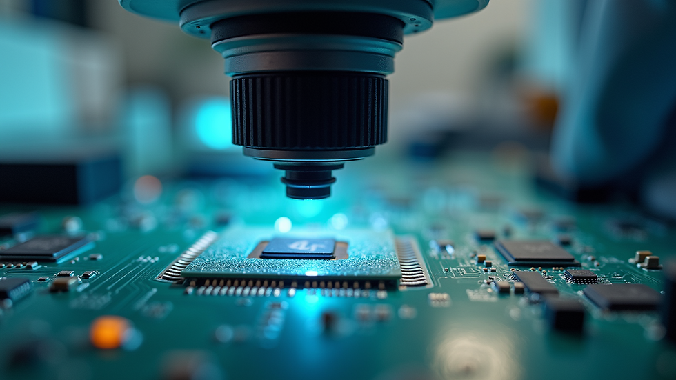
Overcoming Common Challenges in Prototype PCB Assembly
Prototype assembly presents unique challenges. Here are common issues and how to address them:
Component availability: Lead times can delay prototypes. Source critical parts early and consider alternatives.
Soldering defects: Cold joints, bridging, and tombstoning can occur. Optimize solder paste volume and reflow profiles.
Design changes: Rapid design iterations require flexible assembly processes. Use modular designs to minimize rework.
Testing complexity: Functional testing may require custom fixtures. Plan test development alongside assembly.
By anticipating these challenges, you can reduce delays and improve prototype quality.
Leveraging Advanced Technologies in Prototype Assembly
Modern PCB assembly benefits from technological advancements. Consider integrating these into your process:
3D solder paste inspection: Detects paste volume and placement errors before component placement.
Automated optical inspection (AOI): Identifies component misalignment and solder defects quickly.
X-ray inspection: Essential for verifying hidden joints under BGAs and other complex packages.
Rapid prototyping machines: Enable quick turnaround for small batches with high precision.
Adopting these technologies enhances reliability and speeds up development cycles.
Final Thoughts on Mastering Prototype PCB Assembly
Mastering prototype PCB assembly is a strategic advantage. It ensures your designs translate into functional, reliable products. By partnering with expert providers and following best practices, you can streamline development and reduce risks.
For companies in aerospace, medical devices, consumer electronics, and defense, quality and precision are non-negotiable. Leveraging local expertise and advanced technologies positions your projects for success.
Explore trusted options like prototype pcb assembly ventura to access specialized services tailored to your needs. This approach supports your goal of delivering certified, high-quality electronic solutions from design through full production.


Comments